
Procedure
- Step 1: Add a Program Counter
- Add a Program Counter from the Components section.
- Take two input components and connect them to the inputs of the Program Counter.
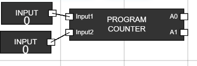
Figure 1: Program Counter with Inputs - Step 2: Add a ROM
- Select a ROM from the Components section.
- Connect the A0 and A1 outputs of the Program Counter to the A0 and A1 inputs of the ROM.
- Add another input component and connect it to the CS (Chip Select) input of the ROM, then rename it to "Clock".
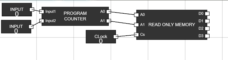
Figure 2: ROM Connected - Step 3: Add an Instruction Register
- Add an Instruction Register from the Components section.
- Connect the outputs (D0, D1, D2, D3) of the ROM to the inputs (A0, A1, A2, A3) of the Instruction Register.
- Add two more input components, rename them as "Store" and "Clock", and connect them to the respective Store and Clock inputs of the Instruction Register.
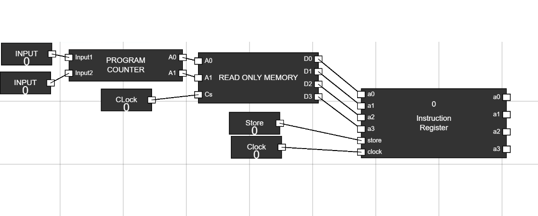
Figure 3: Instruction Register Connected - Step 4: Add a Control Unit
- Add a Control Unit from the Components section.
- Connect the outputs (A0, A1, A2, A3) of the Instruction Register to the inputs (Input1, Input2, Input3, Input4) of the Control Unit.
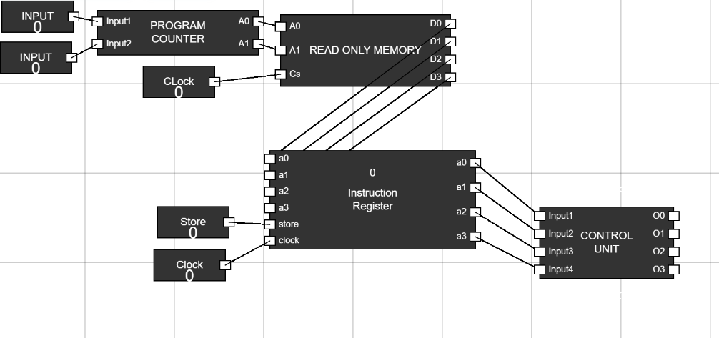
Figure 4: Control Unit Connected - Step 5: Add an ALU
- Add an ALU (Arithmetic Logic Unit) to the workspace.
- Connect the outputs (O0, O1, O2, O3) of the Control Unit to the inputs (S0, S1, S2, S3) of the ALU.
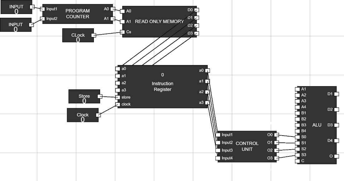
Figure 5: ALU Connected - Step 6: Add Inputs to the ALU
- Take 8 input components and connect them to the inputs (A1, A2, A3, A4, B1, B2, B3, B4) of the ALU.
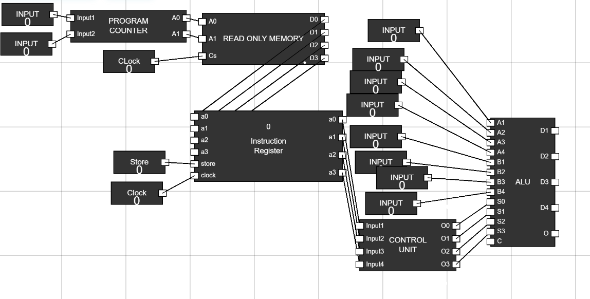
Figure 6: ALU Inputs - Step 7: Add a 4-Bit Register
- Add a 4-bit register to the workspace.
- Connect the inputs (A0, A1, A2, A3) of the register to the outputs (D1, D2, D3, D4) of the ALU.
- Add two additional input components, rename them as "Store" and "Clock", and connect them to the respective inputs of the 4-bit register.
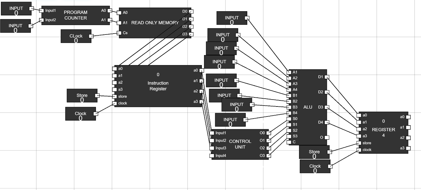
Figure 7: Register Connected - Step 8: Add Outputs
- Add 4 output components and connect them to the outputs (O1, O2, O3, O4) of the 4-bit register.
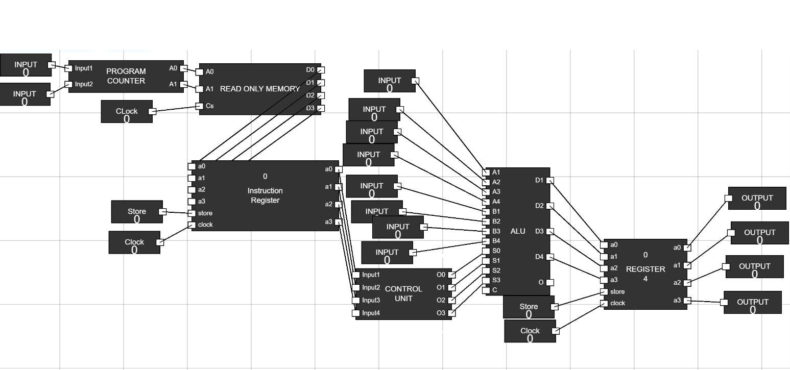
Figure 8: Outputs Connected - Step 9: Set Clock and Store
- Set the values of "Clock" and "Store" inputs to 1.
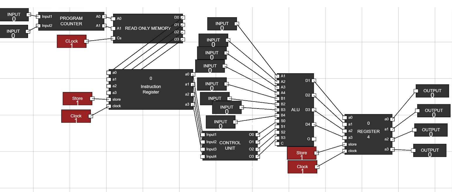
Figure 9: Clock and Store Set - Step 10: Verify Operation
- Set the Program Counter inputs to specific values and observe operations:
- For Input1=0 and Input2=0, Addition is performed in the ALU.
- For Input1=1 and Input2=0, Transfer A operation occurs.
- Verify the results by observing the output of the 4-bit register.
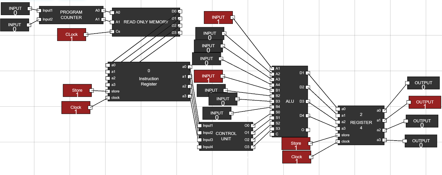
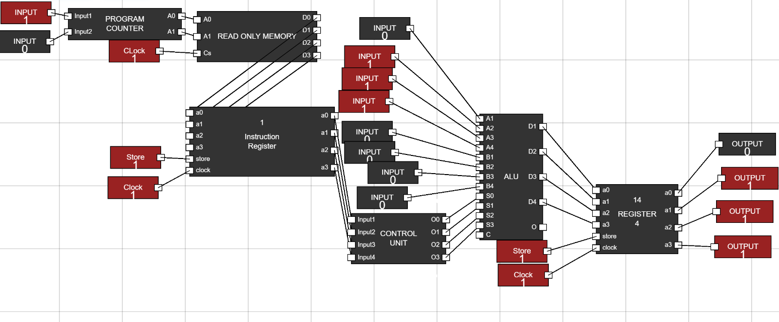
Figure 10: Operation Verified