
Theory
Introduction
In the realm of digital systems, memory is an indispensable component that serves as the repository for data.
To access specific data, a unique address is provided to the memory, directing the system to the desired
location. The process of interpreting this address and selecting the corresponding memory location is known as
memory address decoding.
At the heart of memory address decoding lies a crucial component: the decoder. This digital circuit accepts an
input address, typically in binary format, and generates a unique output signal corresponding to the selected
memory location. The decoder's functionality is akin to a switchboard operator, directing incoming calls
(memory requests) to the appropriate lines (memory locations).
In this experiment, we will delve into the intricacies of memory address decoding by designing and
implementing a simple memory address decoder using fundamental logic gates. By inputting various address
combinations, we will observe how the decoder activates specific output lines, visually representing the
selection of memory locations. This hands-on approach will provide a tangible understanding of the und

Registers:
• Function: Registers are small, fast storage units used to hold data temporarily. In the context of memory addressing, they are used to store the memory address that needs to be accessed.
Working of Registers:
In the experiment, the register plays a vital role in memory address decoding using logic gates. The input data is first fed into the register, which temporarily holds it for processing. The memory address is decoded using logic gates such as OR, NOT, and 3-input NAND gates. These gates process the address lines to select the appropriate memory location in the RAM. The decoded address determines which part of the RAM will be accessed. Once the correct address is identified, the data is either written to or read from the RAM, with the register acting as a temporary storage for holding the data during the decoding and accessing process. This allows for efficient memory management and data retrieval in the microprocessor simulation.
RAM (Random Access Memory):
• Function: RAM is the main memory unit where data is stored. It has a grid-like structure with rows and columns that can be accessed using an address.
• Addressing: The RAM receives address inputs from the decoder and either outputs data from that address (read operation) or accepts data to store at that address (write operation).
• Integration: The RAM is connected to the address decoder and control signals, allowing it to perform read and write operations based on the input conditions.
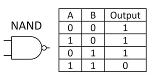
Logic Gates (NAND, OR, NOT):
• NAND Gates: The most fundamental and versatile logic gate. You can build any other logic gate (AND, OR, NOT, XOR) using combinations of NAND gates. NAND gates are often chosen due to their simplicity and availability.
• OR Gates: Used to combine multiple signals or conditions. For example, they can be used in the control logic to manage combined control signals.

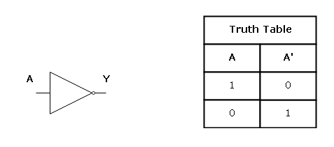
• NOT Gates: Inverts the input signal and is useful for creating complement operations and handling negative logic.
Use Case: These gates are used to construct the address decoder and control circuits that translate the binary address into specific actions in the RAM.
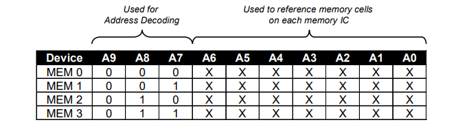
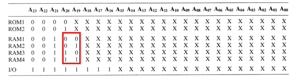
Address Decoder:
• Purpose: The address decoder is essential for translating the binary value from the address register into a specific output line. Each line corresponds to a unique address in the RAM, ensuring that only one memory location is accessed at any time.
• Construction: The decoder can be made from basic logic gates, such as a combination of AND, OR, and NOT gates (or their equivalents built from NAND gates). For example, a 2-to-4 line decoder can convert 2-bit input into one of four outputs.
• Operation: When the binary input from the register is fed into the decoder, it activates a single line corresponding to the memory location in the RAM.
Execution Flow:
1- Input the address to the register.
2- The address is processed by the decoder logic gates.
3- The corresponding output line activates.
4- indicating the selected memory location.
5- (Optional) Control signals manage data read/write if connected to RAM.
Analysis:
• The experiment demonstrates how address decoding works to select specific memory locations based on the input address.
• By changing the address input, the decoder directs the output signal to the corresponding memory location, enabling controlled data access in memory systems.
Conclusion: This experiment illustrates the implementation of a memory address decoding circuit using basic logic gates. It helps understand how digital systems select specific memory addresses for reading or writing data.