
Theory
Introduction
The Data Path Design is fundamental to understanding how data flows through a CPU during instruction execution. It involves key components such as registers, multiplexers, the ALU (Arithmetic Logic Unit), and memory, all coordinated by control signals. The data path executes instructions in stages: Instruction Fetch, Decode, Execute, and Write-Back. Each stage has a unique function, from retrieving and interpreting instructions to performing computations and storing results. This design directly impacts CPU efficiency and performance, providing insight into how processors handle tasks rapidly and accurately, forming a core part of computer architecture studies.
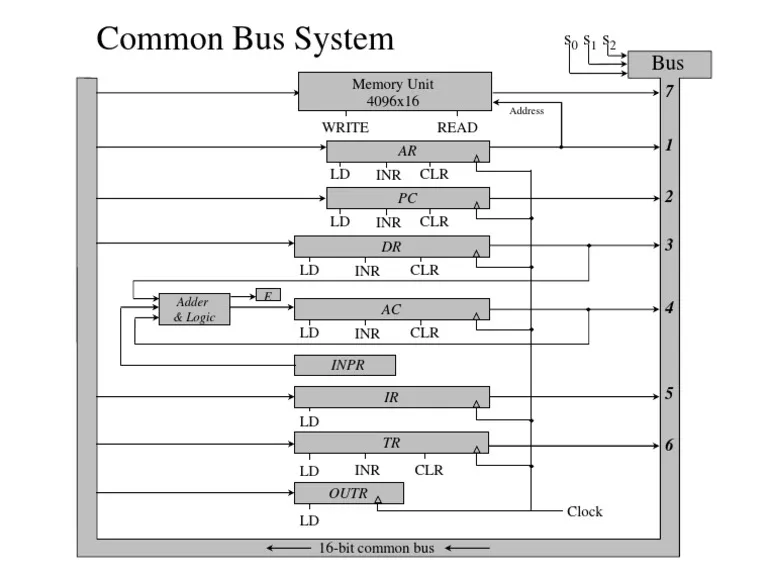
Registers: Registers are small, fast storage units that temporarily hold data or instructions. Common registers include the Program Counter (PC), Instruction Register (IR), and general-purpose registers. Connected to the bus, these registers read and write data as needed during instruction execution, providing quick access to frequently used values.
Working of registers
Registers in data path design play a crucial role in temporarily storing data and facilitating efficient movement between different components of a processor, particularly the ALU. The data transfer process begins with the control unit selecting the appropriate register and enabling it to place its data onto the internal data bus. This data is then fetched by the ALU as input. Once the ALU receives the data, it performs the specified arithmetic or logical operation based on the instruction's opcode. The result generated by the ALU needs to be stored back into a register. The control unit signals the destination register to accept the ALU's output, which is then written back into the register. The entire process is managed through control signals that regulate when a register should output or store data. These signals ensure synchronization between the registers, the ALU, and other components of the data path, making data transfer and processing efficient within a computing system.
Types of Registers
Accumulator (AC): A special register used to store intermediate results of arithmetic and logical operations performed by the ALU. It reduces the need for frequent memory access.Instruction Register (IR): Holds the currently executing instruction fetched from memory. The control unit decodes the instruction stored in this register.
Program Counter (PC): Keeps track of the address of the next instruction to be executed. It is automatically updated after fetching an instruction.
Memory Address Register (MAR): Stores the address of a memory location that is being accessed for either reading data from or writing data to memory.
Memory Data Register (MDR) Holds the actual data being transferred to or from memory. It acts as a buffer between the processor and memory.
ALU (Arithmetic Logic Unit): The ALU performs arithmetic operations (like addition and subtraction) and logical operations (such as AND, OR). It takes inputs from registers via the bus, processes them according to control signals, and outputs results back onto the bus for further use or storage, acting as the primary computation unit.
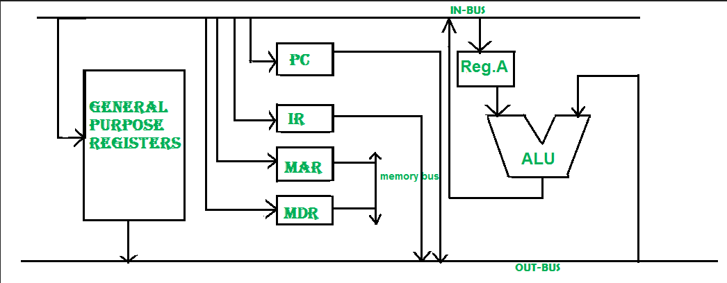
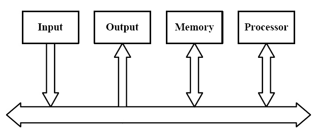
Bus: A bus is a communication pathway that connects multiple components, allowing data transfer among them without direct point-to-point wiring. In the data path, the bus enables flexible data sharing between registers, memory, and the ALU. Control signals govern which component places data on the bus at a given time.
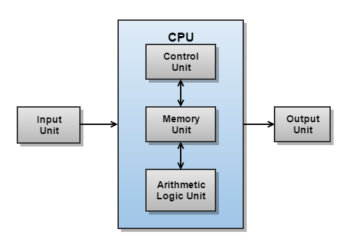
Memory Unit: The memory unit stores data and instructions for the CPU. Through the bus, memory interacts with registers and the ALU, allowing instructions to be fetched, data to be read, and results to be written. The bus enables seamless data exchange, with memory operations directed by control signals for efficient data access.
Data Flow
Data flow in the data path describes how information moves between components during instruction processing. Key elements like registers, the ALU, memory, and buses (or multiplexers) manage this flow. Each instruction initiates a specific data flow path, determined by control signals from the control unit. For instance, during an arithmetic operation, data flows from registers to the ALU, where it is processed and then either stored back in a register or written to memory. Efficient data flow ensures minimal delays and optimized CPU performance, as each component is accessed precisely when needed.
Execution Stages
The data path processes each instruction through a series of execution stages:
Instruction Fetch (IF): In the Instruction Fetch stage, the CPU retrieves the next instruction’s address from the Program Counter (PC) and loads the instruction from memory into the Instruction Register (IR). The PC is then incremented to point to the next instruction, initiating the sequence for the current instruction’s execution.
Decode: During Instruction Decode, the control unit interprets the fetched instruction to determine the operation type, required operands, and control signals. It identifies which registers are needed and prepares the data path components for execution, setting up inputs for the ALU and addressing modes if memory access is required.
Execute: In the Execute stage, the ALU performs the specified operation (e.g., addition, subtraction, logical operations) on the operand data provided by the registers. This stage produces a result based on the instruction’s operation, which is either used directly or prepared for storage or further processing in subsequent stages.
Memory Access(MEM): The Memory Access stage handles data transfer between the CPU and memory. If the instruction involves reading or writing data, the CPU either retrieves data from memory to a register or writes the ALU result to memory, depending on the instruction type, to ensure data availability.
Write-Back: In the Write-Back stage, the final result of the executed instruction is stored back into a destination register or memory location. This step completes the instruction cycle, ensuring that the output is available for use by subsequent instructions, enabling sequential or pipelined execution in the CPU.
Conclusion: Through this experiment, you will understand the role of each component (registers, ALU, and buses) in a basic data path. By simulating data transfer operations, you will also gain insight into how data flows in a computational system, and how registers and ALUs interact in performing computations.
This experiment forms the basis for more complex designs like CPUs, where multiple data paths, control signals, and memory units work together for data processing