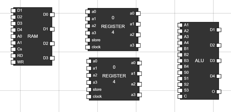
Step 1: Set Up Components:
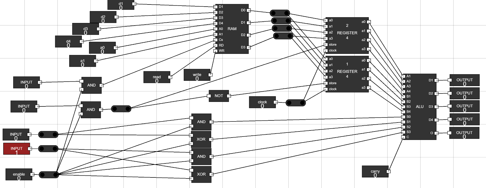
- Navigate to the Components section and add ALU, 2 Registers and a RAM to the workspace. Figure 1: Components in
Worspace
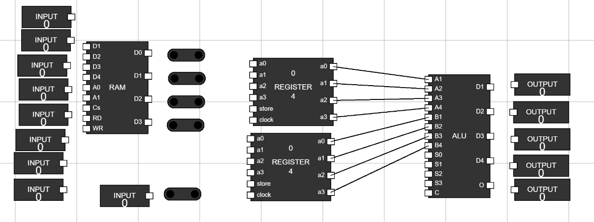
Step 2: Take 9 inputs, 5 junction and 5 outputs to provide inputs to RAM and to show output of ALU:
- Connect the output of first register to first four bit number input of ALU i.e, A1,A2,A3 and A4.
- Connect the output of second register to second four bit number input of ALU i.e, B1,B2,B3 and B4. Figure 2: Add Inputs, Junctions and Outputs
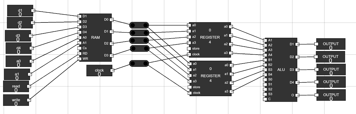
Step 3: Rename and connect Inputs:
- Rename an input by hover over it and clicking CTRL+A. Then enter new name and click ENTER.
- Rename inputs to d1,d2,d3,d4,a0,a1,read,write and clock.
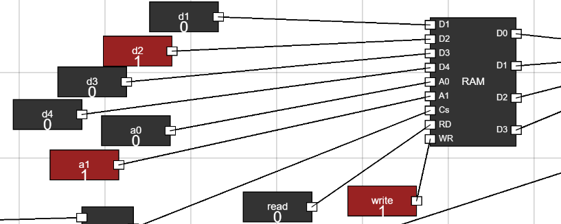
- Connect the inputs d1,d2,d3 and d4 to first four data input of RAM i.e, d1,d2,d3 and d4.
- Connect the inputs a0 and a1 to address bits of RAM a0 and a1.
- Connect the inputs read and write to RD and WR inputs of RAM.
- Place the Junctions in place as shown in figure. Connect the Clock input to a junction and then connect the clock input of both registers to this junction's output.
- Connect output of RAM to four junctions and provide it as data to both Registers at A1,A2,A3 and A4 of both registers.
- Connect the outputs of ALU to the 5 outputs. Figure 3: Renaming and Connecting inputs and outputs
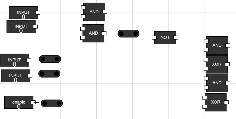
Step 4: Setting up control unit using logic gates:
- Navigate to the Components Section.
- Take 6 inputs, 4 junctions, 4 AND gates, 2 XOR gates and 1 NOT gates. Figure 4: Set up control unit
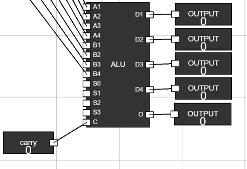
Step 5: Adding Carry input to ALU:
- Rename 1 input to Carry and Connect it to C input of ALU. Figure 5: Add carry input.
Step 6: Place the Components in given format to create Control Unit:
- Rename 1 input to Enable and Connect it to junction to give it as input to all logic gates. Figure 6: Placing components of control unit.
Step 7: Making Connections to gates:
- Connect the enable input to all the logic gates except the NOT gate.
- Connect 1 input to first AND gate.
- Connect 1 input to second AND gate.
- Take the output of second AND gate and connect it to a junction. Then, Connect this junction to the NOT gate.
- Connect the other two inputs to junctions in front of them.
- Connect 1 input through juction to the AND and XOR gate.
- Do the same for last input too. Figure 7: Connections to control unit.
Step 8: Connecting the control inputs to ALU, Registers and RAM:
- Connect output of first AND gate to CS of RAM.
- Connect the output of second AND gate using junction to the store of first regsiter and the output of NOT gate to Store of second register.
- Connect the outputs of AND and XOR gates to the select inputs of ALU i.e, s0,s1,s2 and s3 as shown in figure. Figure 8: Connecting control inputs to ALU, registers and RAM.
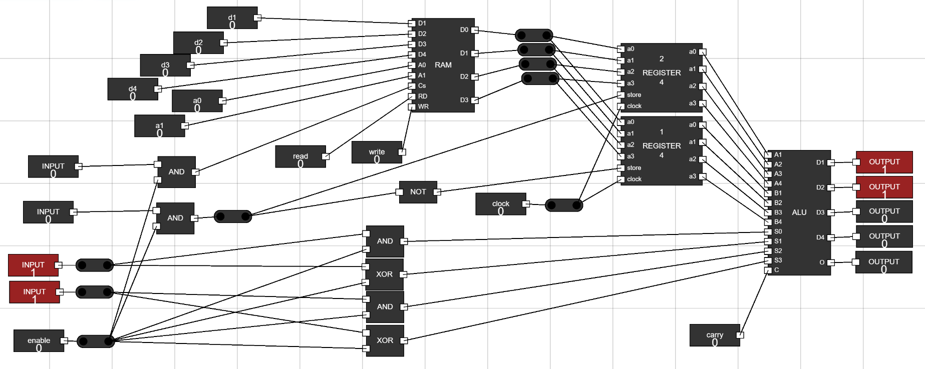
Step 9: Feeding data to RAM:
- Keep the enable input of control unit low.
- In the first four inputs d1,d2,d3 and d4, change them to the number you want to add data to RAM.
- Select the address of RAM using a0 and a1 inputs.
- After selecting the address and data, toggle open the Write input of RAM. Then toggle the Write input of RAM off again.
- Then, select another data and address to store data and toggle open the write input of RAM and then turn it off.
- Now, we have two different data at two different address in our RAM. Figure 9: Feeding data to RAM. Figure 10: Feeding data to RAM.
Step 10: Set up registers to take data:
- Toggle open the clock input of registers to take data from RAM.
- Also, Toggle open the enable and Read of control unit and RAM respectively.
- This will the control word to pass data from the selected address of RAM to the second register from control unit.
- This is a control signal to transfer data to second register and perform addition in ALU. This means that for this particular control word given to control unit i.e, 00001, the control unit generates control signals to perform an operation of transferring data to second register and then performing addition. Figure 11: Transfer Second Register and Addition Control Word.
- Set the enable input to 0.
- Select the second address from RAM using a0 and a1.
- Now change the second input of control unit which is connected to store inputs of registers to select first register.
- Now turn on the enable signal to transfer this data to first register.
- This is another control signal to transfer data to first register and perform addition in ALU. The Control word is (01001).Figure 12: Transfer First Register and Addition Control Word.
- Another control word can be to perform logical AND operation of data present in registers already.
- For this, Toggle off the enable and toggle open the input just above the enable input.
- This is a control word (00010) to perform logical AND on data present in registers.Figure 13: Logical AND Control Word.
- Another control word can be to perform logical OR operation of data present in registers already.
- For this, Toggle off the enable and toggle open the two inputs just above the enable input.
- This is a control word (00110) to perform logical AND on data present in registers.Figure 14: Logical OR Control Word.
Design a control unit for a simple instruction set using logic gates.