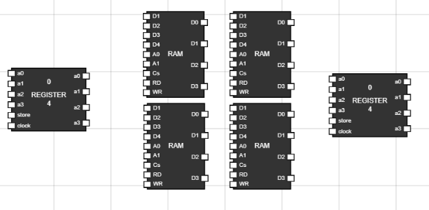
Step 1: Set Up Components:
- Navigate to the Components section and add 4 RAM, 2 Registers to the workspace. Figure 1: Components in
Worspace
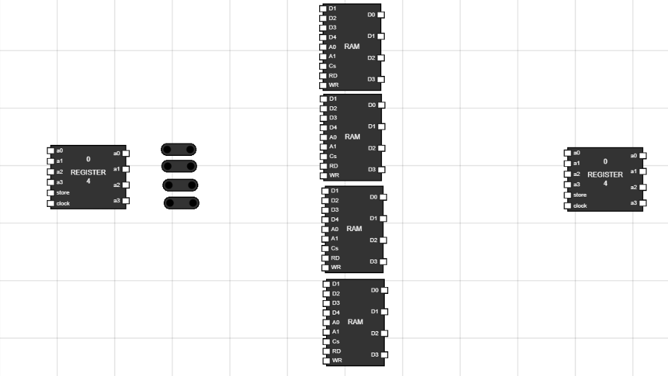
Step 2: Take 4 Junctions to distribute the same data to all RAM's:
- Take 4 junctions from components section. Figure 2: Add junctions
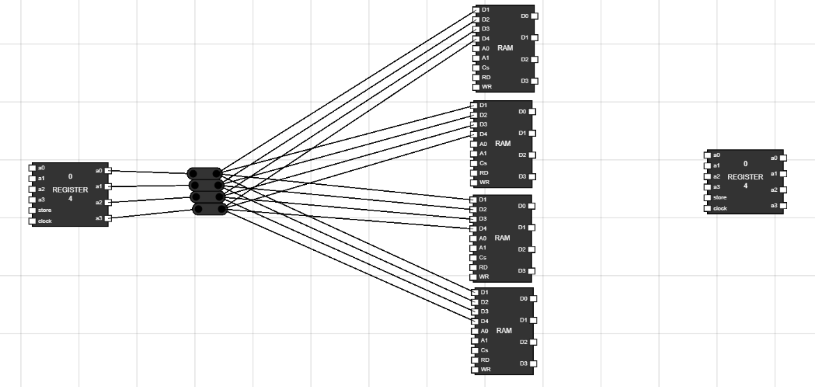
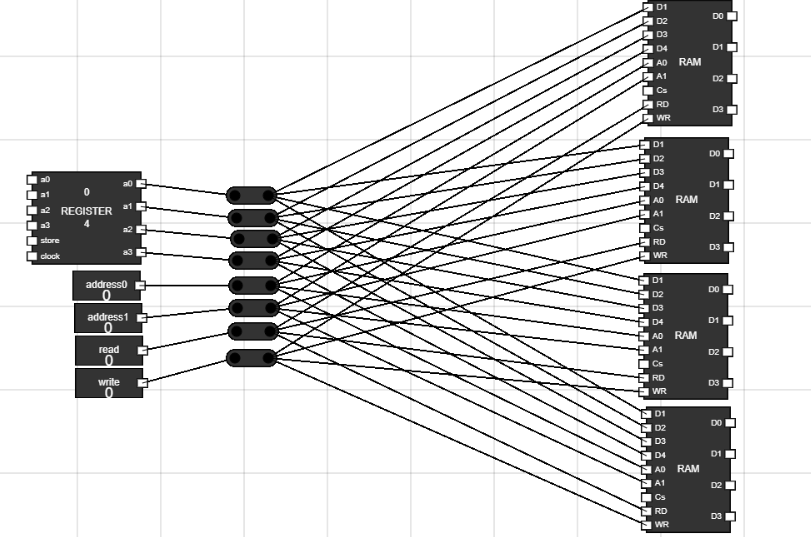
Step 3: Connect outputs from Register to the four juctions and give input to RAM's :
- Connect 4 output of Register to the 4 junctions.
- The data bits of RAM (d1,d2,d3,d4) are used to give data to RAM.
- Connect the junction output to the data input of all 4 RAM's using the 4 junctions. Figure 3: Data input to RAM's
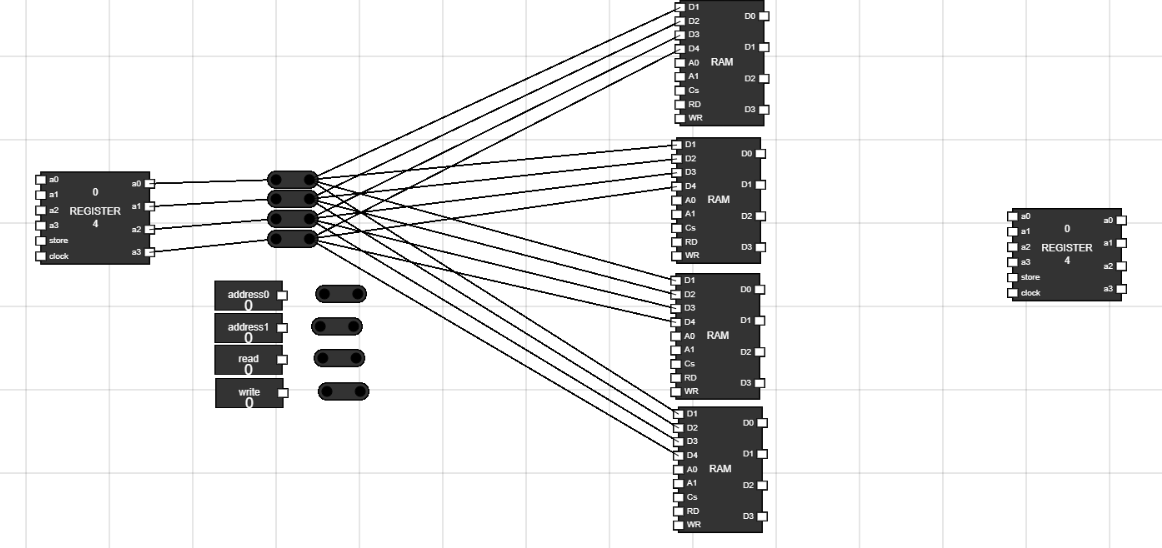
Step 4: Take 4 inputs and 4 junctions on workspace :
- Rename the input by Hover over the input and CTRL+A.
- Rename two inputs with addresss0 and address1.
- Rename other two inputs with Read and Write. Figure 4: More Components
Step 5: Connect address bits and read, write to RAM's :
- Connect these 4 junctions to address bits and read/write input.
- Connect the address bits junction to a0 and a1 of all 4 RAM.
- Connect the read input junction to RD of all 4 RAM.
- Connect the write input junction to WR of all 4 RAM. Figure 5: Connecting RAM address bits and READ/WRITE
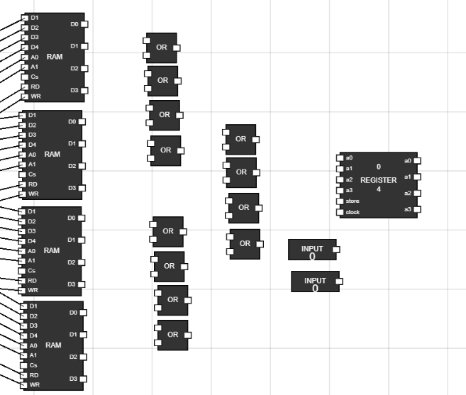
Step 6: Take 12 OR gates, 2 inputs from components :
- Place the OR gates and inputs as shown in figure. Figure 6: Setting up OR gates
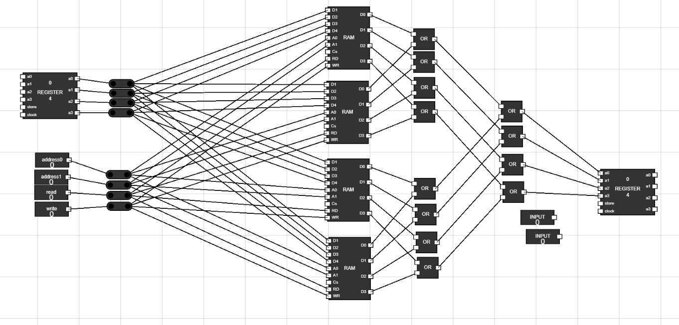
Step 7: Connect the OR gates :
- These OR gates will provide the same data path from all 4 RAM's.
- For first two RAM's, take 4 OR gates.
- Output of first RAM are connected to first input terminals of 4 OR gates respectively.
- Similarly, output of second RAM are connected to second input terminals of 4 OR gates respectively.
- Same OR gate should have the output of same numbered bit from either RAM.
- Do the same thing for other two RAM using 4 OR gates.
- Now, we have two sets of 4 OR gates. Say group1 and group2.
- Now, take four more OR gates, whose first input terminal are connected to group1 OR gates output in numbered fashion.
- The second input terminals of these 4 OR gates are connected to output of group2 OR gates.
- The output of these OR gates are now connected to the register to read the value of data. Figure 7: Connecting OR gates
Step 8: Rename the inputs and connect them to register :
- Rename these inputs to store and clock.
- Connect store input to store of register and clock input to clock of register.
- With this, our memory unit is ready. Now we need a decoder to select a RAM using some input bits. Figure 8: Connecing Output Register
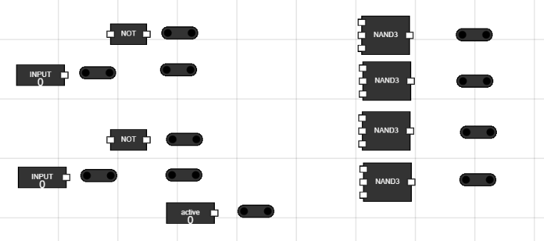
Step 9: Setting up components for 2 X 4 decoder :
- Take 3 inputs, 4 NAND gates, 2 NOT gates and 11 junctions to the workspace.
- Rename one of the input to active, which will switch ON the decoder.
- Place them on workspace as shown in figure. Figure 9: Components for 2 X 4 decoder
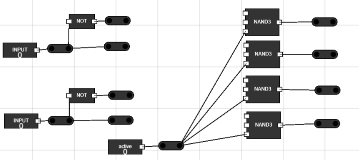
Step 10: Make connections in decoder :
- Connect the inputs to junctions in front of them to send same signal to more than one place.
- Connect the NOT gates input to the two data bits from junctions. Now send the data further from the NOT gates to two more junctions.
- Connect the active signal to last input terminal of all 4 NAND gates.
- Connect the Output of NAND gates to junctions in front of them. Figure 10: Connections in decoder
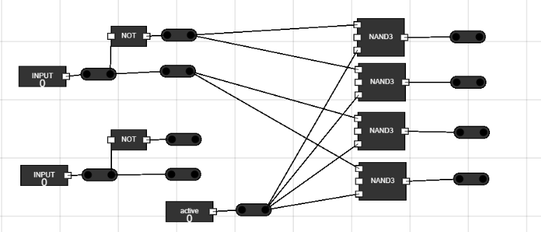
Step 11: Connecting first input and its negative to the NAND gates :
- Say we call the first input as A.
- The junction directly connected to input is A.
- The junction connected to NOT gate in A-.
- Connect first two NAND gates to A-.
- Connect last two NAND gates to A. Figure 11: Connecting inputs to NAND gates
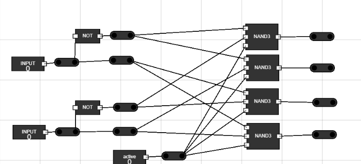
Step 12: Connecting second input and its negative to the NAND gates :
- Say we call the second input as B.
- The junction directly connected to input is B.
- The junction connected to NOT gate in B-.
- Connect first and third NAND gates to B-.
- Connect second and last NAND gates to B. Figure 12: Connecting inputs to NAND gates
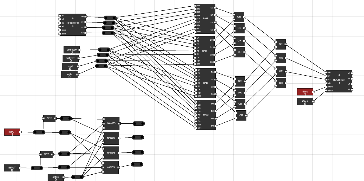
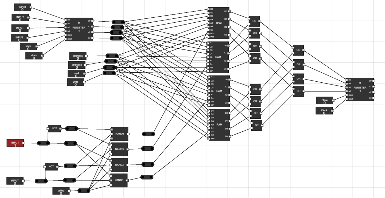
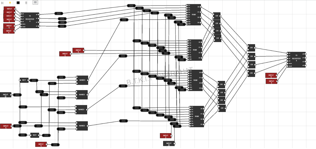
Step 13: Set up looks like this now : Figure 13: Complete setup
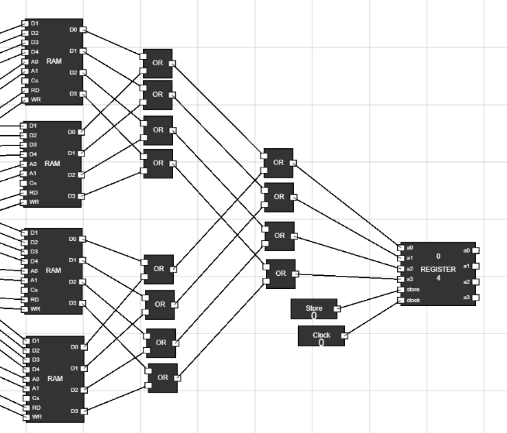
Step 14: Set up the input for first Data register :
- Take 6 inputs from component section.
- Rename two of them to store and clock.
- Connect them to the first register.
- Connect the Output of NAND gates to the CS(chip select) of 4 RAM's.
- Connect them as shown in figure.
Figure 14: Set input for input register and connect the CS of RAM's
- The below table shows which RAM will be selected based on which select input
A
B
RAM number(from top)
0
0
1
0
1
2
1
0
3
1
1
4
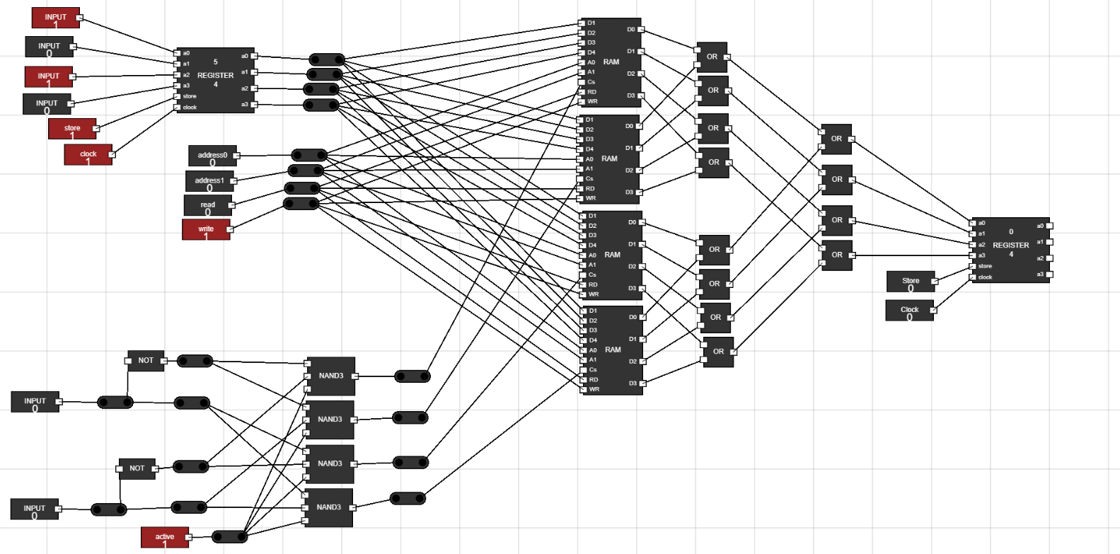
Step 15: How to simulate :
- Select the RAM by the two input bits of decoder.
- After selecting RAM, Set the data in first register to be send to all four RAM's together.
- Store the data in register by switching ON the register with store and clock input.
- Set the address bits for RAM's.
- Set the RAM Write input to 1 to store this data to selected RAM's selected address location.
- Similarly you can set data to different RAM, at different locations.
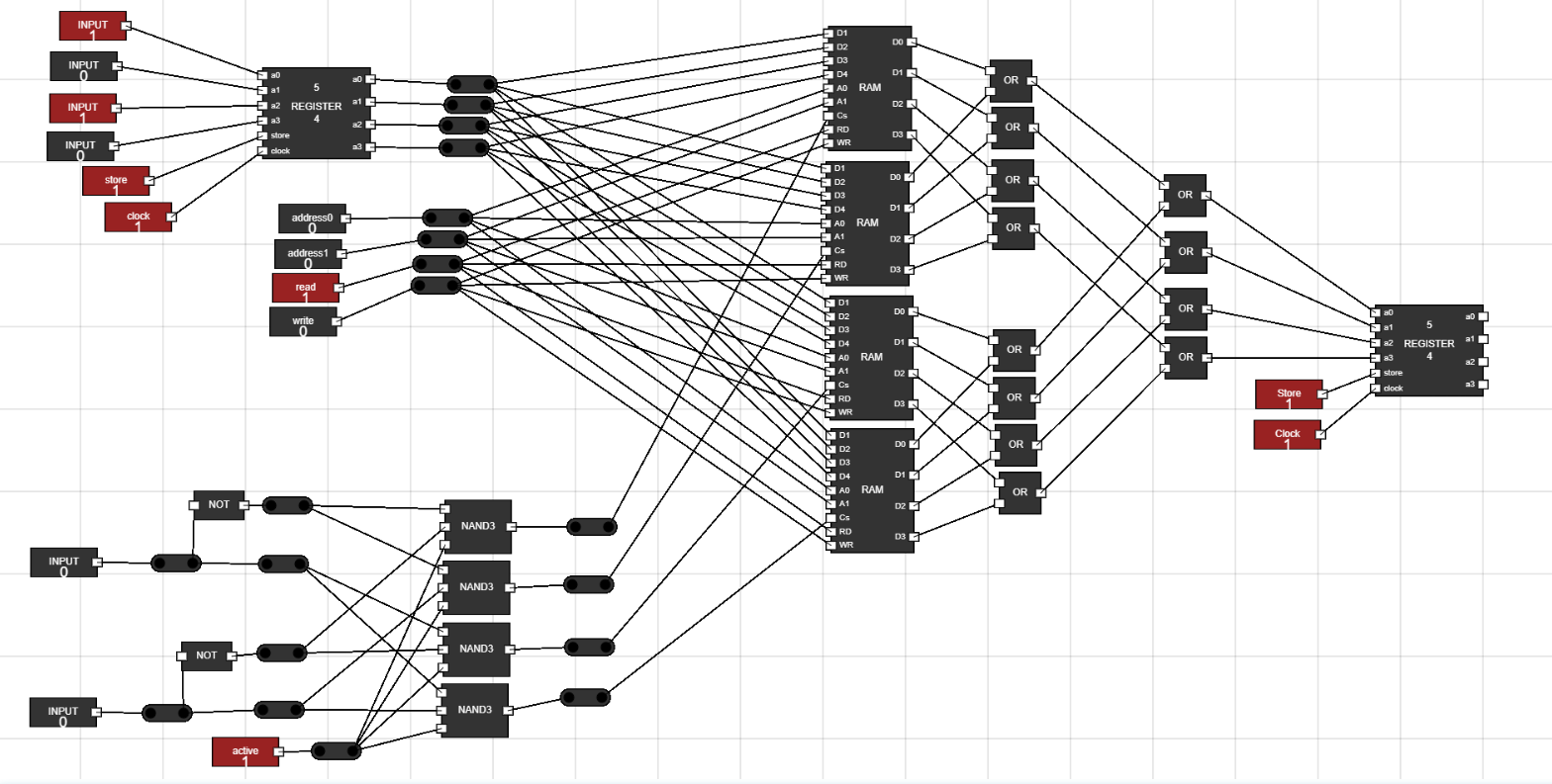
- Now to read this data at output register, make its store and clock input to 1.
- Now switch ON the READ input for the RAM's.
- The stored data will be shown at output. Figure 15: Write Data to RAM's
Figure 16: Access Data from RAM's
Step 16: What comes next :
- Chane the inputs of decoder to select another RAM and check how this circuit works to decode which RAM or memory to select from using 2 bits.
- The circuit can be made more clear with use of more junctions. Figure 17: Cleaner version of Memory address decoder
Implement memory address decoding using logic gates