Procedure for experiment:
- Step 1: Set Up Components:
Navigate to the Components section and click on the BUS,ALU,Register button to add them to the workspace.
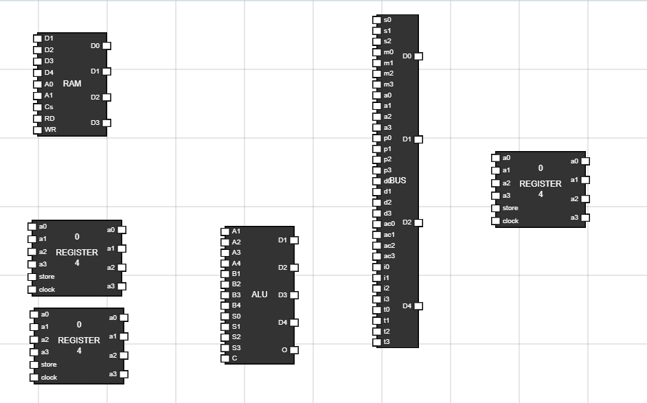
Figure 1: Components in Worspace - Step 2: Set Up Memory Unit(RAM):
Navigate to the Components section and get 9 input button and 4 output to the workspace.
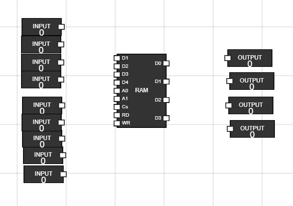
Figure 2: RAM, input and output on workspace - Step 3: Connect inputs to RAM and outputs from RAM. Rename the inputs :
- To reaname the input, hover over that input and click CTRL + A. Then type the new name as shown in figure.
- Connect the inputs to RAM. Make sure to keep CS signal low(0) as it activates RAM.
- Connect the output nodes of RAM to the four outputs.
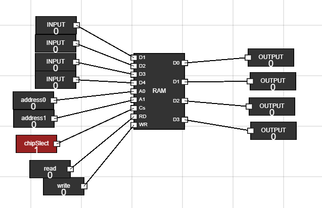
Figure 3: Connections of RAM - Step 4: Write Data into RAM :
- Change the input data as you want to feed into RAM using first four inputs.
- Activate the RAM by making CS low(0).
- Change the address input to where you want to store data.
- Make the write input of RAM high(1).
- Close the CS. Now change the data and address and then again make the CSlow (0) to write the data. - Now do the same to change data at other address locations i.e, at 00, 01, 10 and 11 address locations
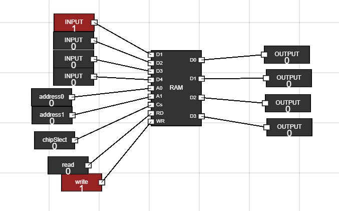
Figure 4: Write data to RAM - Step 5: Read Data from RAM :
- Activate the RAM by making CS low(0).
- Change the address input from where you want to read data.
- Make the read input of RAM high(1).
- You can see the data into output fields.
- Now do the same to read data from other address locations i.e, at 00, 01, 10 and 11 address locations
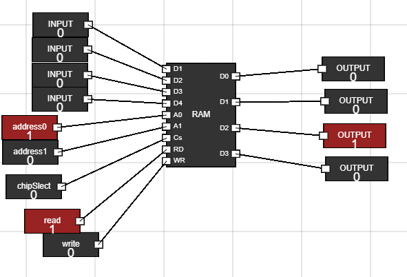
Figure 5: Read data from RAM - Step 6: Remove the output :
- Remove the output buttons by clicking on them and then click on delete key.
- We are doing this as we need to connect output of RAM to the BUS instead of directly displaying output.
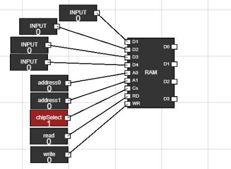
Figure 6: RAM complete setup - Step 7: Set up ALU, Accumulator(register) and Data Register(register) :
- Take the ALU, and two registers to the workspace.
- The register at top is treated as Accumulator.
- The register at bottom is treated as Data Register.
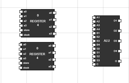
Figure 7: Setup ALU, Accumulator and Data Register - Step 8: Set up inputs and outputs for registers and ALU :
- Take 8 inputs, one pulse and one +ve edge trigger.
- Take 1 output.This is used to display Overflow bit.
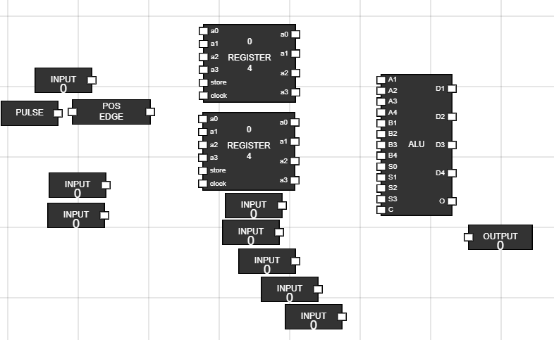
Figure 8: Inputs and output for ALU section - Step 9: Rename the input and connect them to registers and ALU :
- Connect the store and pulse input to Accumulator.
- Connect the store and clock to Data register.
- Connect the output of Accumulator and Data Register to data input of ALU i.e, first 8 pins.
- Connect select lines to ALU and one carry input.
- Also connect the overflow bit of ALU to the output node.
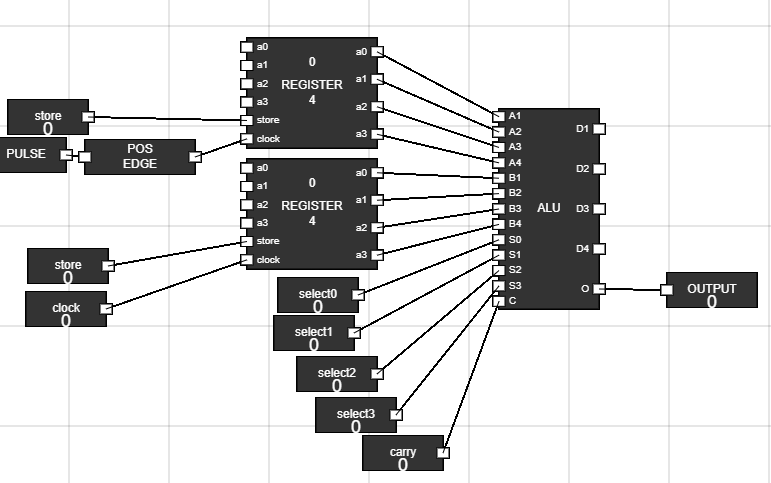
Figure 9: Connected inputs to ALU and Registers - Step 10: Take 8 junctions :
- Output of ALU is only connected to Accumulator. To create this path we use 8 juctions.
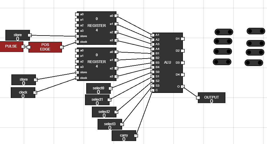
Figure 10: Added Junctions - Step 11: Connecting ALU output to junctions :
- Connect output of ALU to junctions above it. Now connect the output of these junctions to input of the other four junctions.
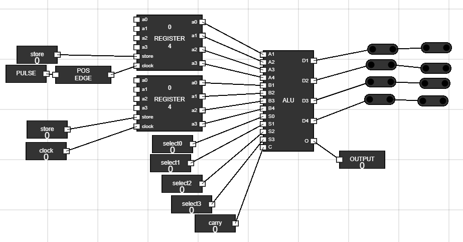
Figure 11: ALU output to junctions - Step 12: Connecting ALU output to Accumulator input :
- Place the juctions on workspace as shown.
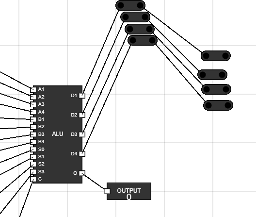
Figure 12: Juncitons placement 1
- Now move the other 4 junctions to the back of Accumulator.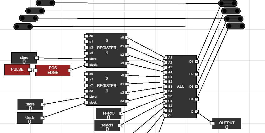
Figure 13: Junctions placement 2
- Now connect the output of these junctions to the Accumulator input.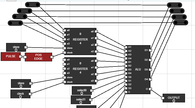
Figure 14: ALU to Accumulator connection - Step 13: Set up the BUS component :
- Take the Bus component.
- Now, take 3 input and rename them to select0, select1 and select2 respectively.
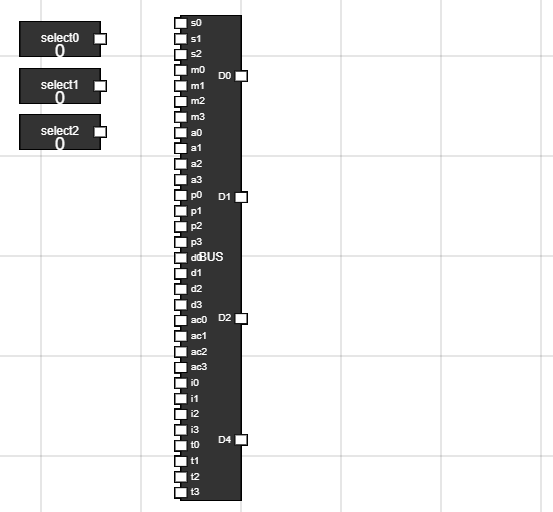
Figure 15: BUS component setup - Step 14: Connect These inputs to select inputs of BUS :
- Connect select inputs to S0, S1 and S2 of BUS.
- In BUS there are 8 groups of 4 bit input.
- These inputs will be selected on basis of S0, S1, and S2.
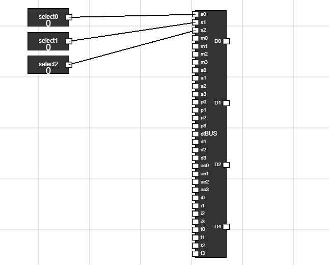
Figure 16: Select input of BUS
- The below table shows which input will be selected based on which select input
S0 S1 S2 Component Selected 0 0 0 Memory Unit(M0,M1,M2 and M3) 0 0 1 Address Register 0 1 0 Program Counter 0 1 1 Data Register 1 0 0 Accumulator 1 0 1 Instruction Register 1 1 0 Temporary Register 1 1 1 All 0's
- Step 15: Connect the output of RAM(memory) to the bus :
- Connect the output of RAM to the m0,m1,m2 and m3 input of BUS.
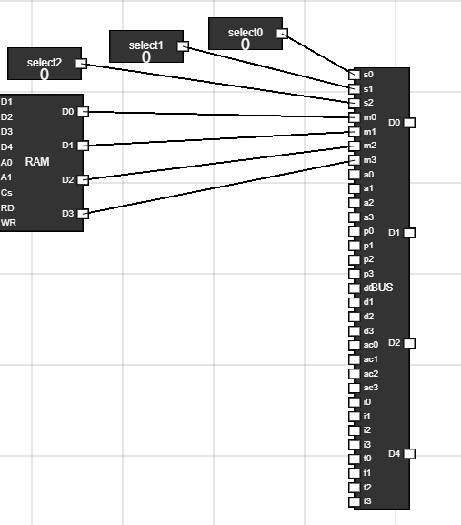
Figure 17: RAM and BUS connection - Step 16: The complete workspace should look like this :
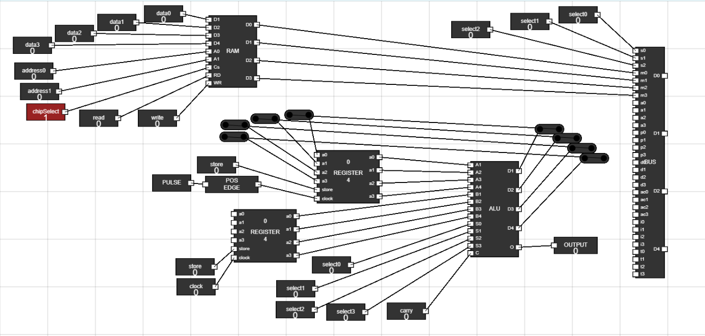
Figure 18: Overview - Step 17: Add 12 junctions to workspace :
- Add 12 junctions to workspace from components bar.
- Connect the output of BUS to four junctions.
- Connect rest of the junctions as shown in figure.
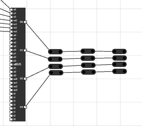
Figure 19: Add junctions - Step 18: Place the junctions on workplace as shown in figure :
- Use thes images to set the position of the junctions.
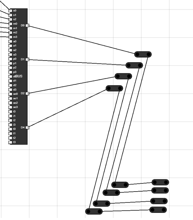
Figure 20: Junctions placement 1
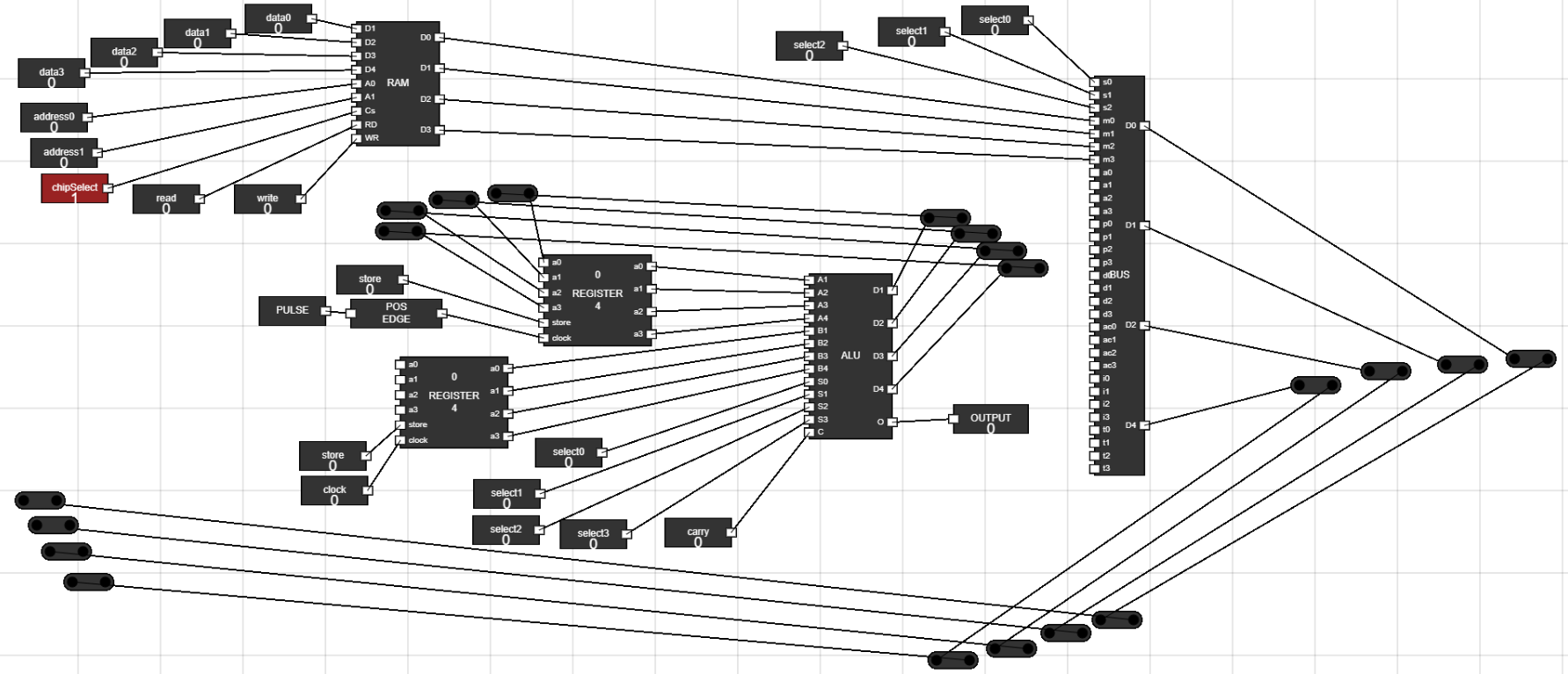
Figure 21: Junctions placement 2 - Step 19: Connect the output of juctions to input of Data Register :
- Connect the output of BUS using junctions to the input of Data Register.
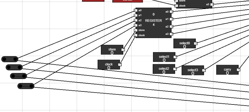
Figure 22: Connect BUS to Data Register - Step 20: The Complete Setup for experiment looks like :
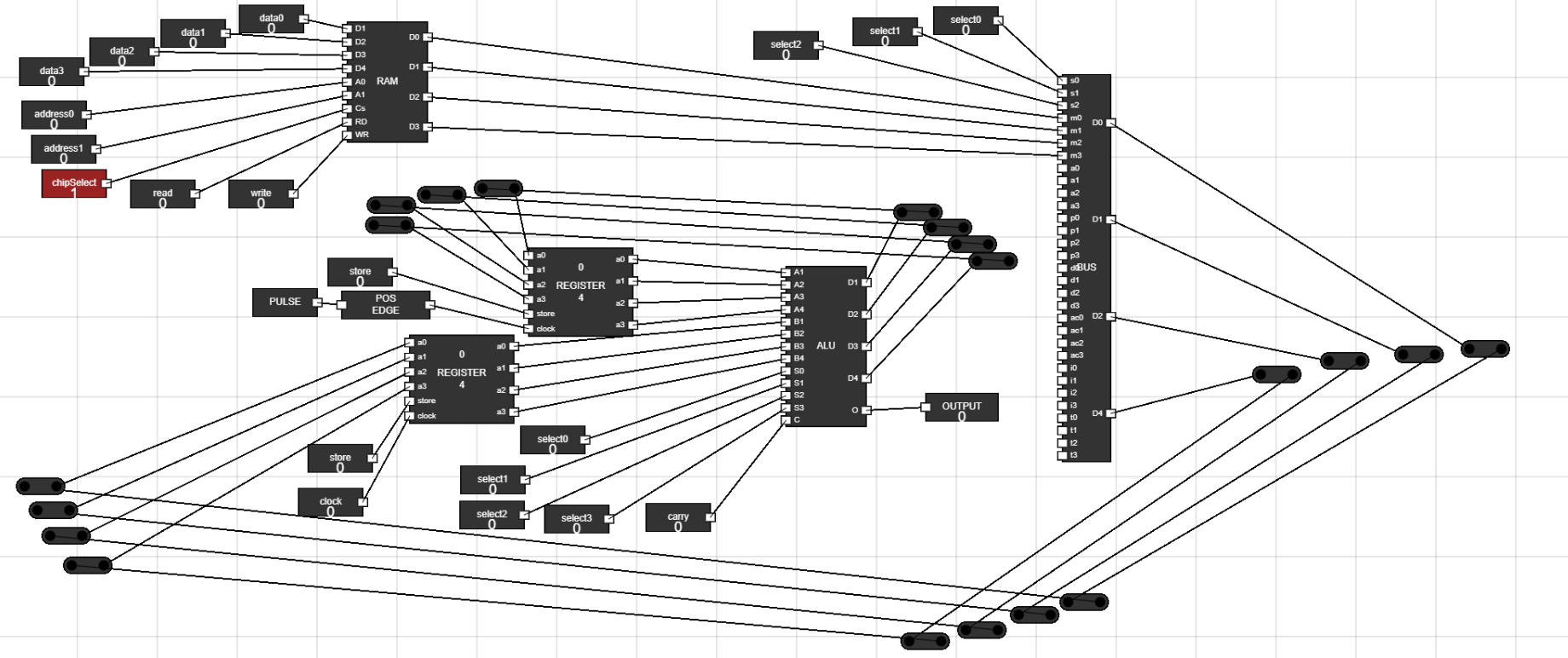
Figure 23: Complete Setup - Step 21: How to Simulate the Data Path in Computer :
- Suppose, You want to add two 4 bit data.
- Using address bit input of RAM select the address of data you want as first operand.
- Make the CS input of RAM low(0) and Read input of RAM high(1).
- To select RAM or memory in BUS, keep the value of select inputs of BUS as 000.
- Now, BUS has the first 4 bit data we want as operand.
- To use this data in ALU operation, we need to get it into the Data Register.
- To take the data into Data Register, set the store and clock input of Data Register high(1).
- Once you have data into Data Register, set its clock and store input as 0 to not change the value it holds further if data in BUS changes.
- Now trasfer this data to Accumulator using select inputs of ALU.
- Keep all select inputs of ALU as 0 and carry as 0. This will lead to a arithmetic addition without carry and as the Accumulator initially has zero, a Transfer B operation will be performed.
- Now to store the processed data into Accumulator, you need to set the clock pulse and +ve edge trigger to slow speed by clicking on them till the blinking speed is least. This is because the ALU works continuosly and will perform the operation over and over.
- Toggle the store input of Accumulator to high(1) and as soon as you get data inside it from ALU, toggle the Store input of Accumulator again to low(0) to not let the data inside it change again.
- Now, bring another data from any address location in RAM to the Data Register.
- Keeping the ALU inputs to 0, ALU will perform Arithmetic Addition without carry and will add data in Accumulator and Data Register.
- To store this Data into Accumulator again, toggle open the Store input of Accumulator.
- As soon as data is updated in Accumulator, turn the store input of Accumulator to 0.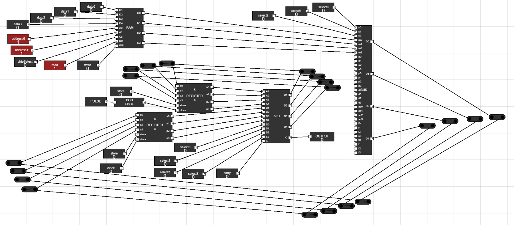
Figure 24: Result of Experiment - Step 22: Connect the output of juctions to input of Data Register :
- If you want to store this processed data into the memory again, then you would need to connect the BUS output to RAM also like Data Register.
- Also, Connect this accumulator output to the BUS at ac0,ac1,ac2 and ac3.
- Select the accumulator in BUS using appropriate select input for BUS.
- Then store the data back into the RAM using the output of BUS.
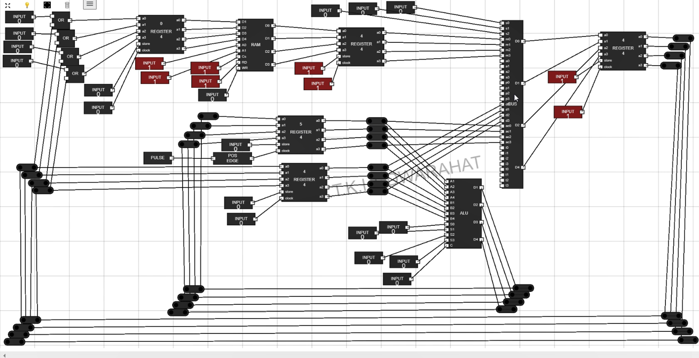
Figure 25: What comes Next